中+8613161801490
| Crystal | |
|---|---|
| 1.1 Growing Method | MOCVD |
| 1.2 Orientation | <111> crystal orientation |
| 1.3 thickness | 5~5.5um |
| 1.4 Surface coverage/thickness | GaN /2-2.5nm |
| 1.5GaN quality | <600”(002 ) |
| <1000”(102) | |
| 1.6 HEMT component |
AlxGal-xN,0.2 |
| 1.7 ALN intermediate layer | 1-2nm |
| Electrical | |
| Two-dimensional electron gas concentration of HEMT structure | >8E12/cm² |
| Mechanical | |
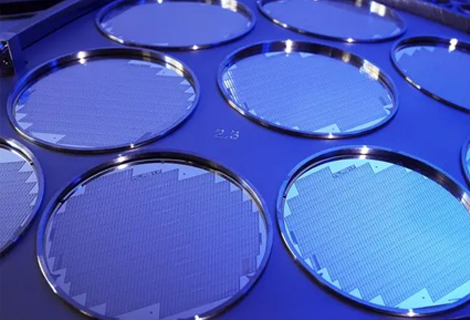
| Diameter | 150±0.2mm |
| Surface Treatment | |
| Crack (Edge 5 mm) | without |
| Surface Treatment | |
|---|---|
| Crack (Edge 5 mm) | without |
Add:Room 219, 2nd Floor, Building 23, Wenzhou National University Science Park, No. 89 Fengfang Road, Ouhai Economic Development Zone
Tel:+8613161801490E-Mail:154330064@qq.com